A carbon nanotube (CNT) is a tube made of carbon with diameters typically measured in nanometres.


Single-wall carbon nanotubes (SWCNTs) Single-wall carbon nanotubes are one of the allotropes of carbon, intermediate between fullerene cages and flat graphene, with diameters in the range of a nanometre. Although not made this way, single-wall carbon nanotubes can be idealized as cutouts from a two-dimensional hexagonal lattice of carbon atoms rolled up along one of the Bravais lattice vectors of the hexagonal lattice to form a hollow cylinder. In this construction, periodic boundary conditions are imposed over the length of this roll-up vector to yield a helical lattice of seamlessly bonded carbon atoms on the cylinder surface.[1]
Multi-wall carbon nanotubes (MWCNTs) consisting of nested single-wall carbon nanotubes[1] weakly bound together by van der Waals interactions in a tree ring-like structure. If not identical, these tubes are very similar to Oberlin, Endo, and Koyama's long straight and parallel carbon layers cylindrically arranged around a hollow tube.[2] Multi-wall carbon nanotubes are also sometimes used to refer to double- and triple-wall carbon nanotubes.
Carbon nanotubes can also refer to tubes with an undetermined carbon-wall structure and diameters less than 100 nanometres. Such tubes were discovered in 1952 by Radushkevich and Lukyanovich.[3][4]
The length of a carbon nanotube produced by common production methods is often not reported, but is typically much larger than its diameter. Thus, for many purposes, end effects are neglected and the length of carbon nanotubes is assumed infinite.
Carbon nanotubes can exhibit remarkable electrical conductivity,[5][6] while others are semiconductors.[7][8] They also have exceptional tensile strength[9] and thermal conductivity[10][11][12] because of their nanostructure and strength of the bonds between carbon atoms. In addition, they can be chemically modified.[13] These properties are expected to be valuable in many areas of technology, such as electronics, optics, composite materials (replacing or complementing carbon fibers), nanotechnology, and other applications of materials science.
Rolling up a hexagonal lattice along different directions to form different infinitely long single-wall carbon nanotubes shows that all of these tubes not only have helical but also translational symmetry along the tube axis and many also have nontrivial rotational symmetry about this axis. In addition, most are chiral, meaning the tube and its mirror image cannot be superimposed. This construction also allows single-wall carbon nanotubes to be labeled by a pair of integers.[7]
A special group of achiral single-wall carbon nanotubes are metallic,[5] but all the rest are either small or moderate band gap semiconductors.[7] These electrical properties, however, do not depend on whether the hexagonal lattice is rolled from its back to front or from its front to back and hence are the same for the tube and its mirror image.[7]
The remarkable properties predicted for SWCNTs were tantalizing, but a path to creating them was lacking until 1993, when Iijima and Ichihashi at NEC and Bethune et al. at IBM independently discovered that co-vaporizing carbon and transition metals such as iron and cobalt could specifically catalyze SWCNT formation.[14][15] These discoveries triggered research that succeeded in greatly increasing the efficiency of the catalytic production technique,[16] and led to an explosion of work to characterize and find applications for SWCNTs.
Structure of SWNTs


Basic details


The structure of an ideal (infinitely long) single-walled carbon nanotube is that of a regular hexagonal lattice drawn on an infinite cylindrical surface, whose vertices are the positions of the carbon atoms. Since the length of the carbon-carbon bonds is fairly fixed, there are constraints on the diameter of the cylinder and the arrangement of the atoms on it.[17]
In the study of nanotubes, one defines a zigzag path on a graphene-like lattice as a path that turns 60 degrees, alternating left and right, after stepping through each bond. It is also conventional to define an armchair path as one that makes two left turns of 60 degrees followed by two right turns every four steps. On some carbon nanotubes, there is a closed zigzag path that goes around the tube. One says that the tube is of the zigzag type or configuration, or simply is a zigzag nanotube. If the tube is instead encircled by a closed armchair path, it is said to be of the armchair type, or an armchair nanotube. An infinite nanotube that is of the zigzag (or armchair) type consists entirely of closed zigzag (or armchair) paths, connected to each other.
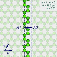
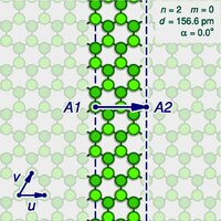
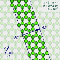
The zigzag and armchair configurations are not the only structures that a single-walled nanotube can have. To describe the structure of a general infinitely long tube, one should imagine it being sliced open by a cut parallel to its axis, that goes through some atom A, and then unrolled flat on the plane, so that its atoms and bonds coincide with those of an imaginary graphene sheet—more precisely, with an infinitely long strip of that sheet. The two halves of the atom A will end up on opposite edges of the strip, over two atoms A1 and A2 of the graphene. The line from A1 to A2 will correspond to the circumference of the cylinder that went through the atom A, and will be perpendicular to the edges of the strip. In the graphene lattice, the atoms can be split into two classes, depending on the directions of their three bonds. Half the atoms have their three bonds directed the same way, and half have their three bonds rotated 180 degrees relative to the first half. The atoms A1 and A2, which correspond to the same atom A on the cylinder, must be in the same class. It follows that the circumference of the tube and the angle of the strip are not arbitrary, because they are constrained to the lengths and directions of the lines that connect pairs of graphene atoms in the same class.
Let u and v be two linearly independent vectors that connect the graphene atom A1 to two of its nearest atoms with the same bond directions. That is, if one numbers consecutive carbons around a graphene cell with C1 to C6, then u can be the vector from C1 to C3, and v be the vector from C1 to C5. Then, for any other atom A2 with same class as A1, the vector from A1 to A2 can be written as a linear combination n u + m v, where n and m are integers. And, conversely, each pair of integers (n,m) defines a possible position for A2.[17] Given n and m, one can reverse this theoretical operation by drawing the vector w on the graphene lattice, cutting a strip of the latter along lines perpendicular to w through its endpoints A1 and A2, and rolling the strip into a cylinder so as to bring those two points together. If this construction is applied to a pair (k,0), the result is a zigzag nanotube, with closed zigzag paths of 2k atoms. If it is applied to a pair (k,k), one obtains an armchair tube, with closed armchair paths of 4k atoms.
Types


Moreover, the structure of the nanotube is not changed if the strip is rotated by 60 degrees clockwise around A1 before applying the hypothetical reconstruction above. Such a rotation changes the corresponding pair (n,m) to the pair (−2m,n+m). It follows that many possible positions of A2 relative to A1 — that is, many pairs (n,m) — correspond to the same arrangement of atoms on the nanotube. That is the case, for example, of the six pairs (1,2), (−2,3), (−3,1), (−1,−2), (2,−3), and (3,−1). In particular, the pairs (k,0) and (0,k) describe the same nanotube geometry. These redundancies can be avoided by considering only pairs (n,m) such that n > 0 and m ≥ 0; that is, where the direction of the vector w lies between those of u (inclusive) and v (exclusive). It can be verified that every nanotube has exactly one pair (n,m) that satisfies those conditions, which is called the tube's type. Conversely, for every type there is a hypothetical nanotube. In fact, two nanotubes have the same type if and only if one can be conceptually rotated and translated so as to match the other exactly. Instead of the type (n,m), the structure of a carbon nanotube can be specified by giving the length of the vector w (that is, the circumference of the nanotube), and the angle α between the directions of u and w, which may range from 0 (inclusive) to 60 degrees clockwise (exclusive). If the diagram is drawn with u horizontal, the latter is the tilt of the strip away from the vertical.
Chirality and mirror symmetry
A nanotube is chiral if it has type (n,m), with m > 0 and m ≠ n; then its enantiomer (mirror image) has type (m,n), which is different from (n,m). This operation corresponds to mirroring the unrolled strip about the line L through A1 that makes an angle of 30 degrees clockwise from the direction of the u vector (that is, with the direction of the vector u+v). The only types of nanotubes that are achiral are the (k,0) "zigzag" tubes and the (k,k) "armchair" tubes. If two enantiomers are to be considered the same structure, then one may consider only types (n,m) with 0 ≤ m ≤ n and n > 0. Then the angle α between u and w, which may range from 0 to 30 degrees (inclusive both), is called the "chiral angle" of the nanotube.
Circumference and diameter
From n and m one can also compute the circumference c, which is the length of the vector w, which turns out to be:

in picometres. The diameter 


also in picometres. (These formulas are only approximate, especially for small n and m where the bonds are strained; and they do not take into account the thickness of the wall.)
The tilt angle α between u and w and the circumference c are related to the type indices n and m by:

where arg(x,y) is the clockwise angle between the X-axis and the vector (x,y); a function that is available in many programming languages as atan2(y,x). Conversely, given c and α, one can get the type (n,m) by the formulas:
which must evaluate to integers.
Physical limits
Narrowest examples

If n and m are too small, the structure described by the pair (n,m) will describe a molecule that cannot be reasonably called a "tube", and may not even be stable. For example, the structure theoretically described by the pair (1,0) (the limiting "zigzag" type) would be just a chain of carbons. That is a real molecule, the carbyne; which has some characteristics of nanotubes (such as orbital hybridization, high tensile strength, etc.) — but has no hollow space, and may not be obtainable as a condensed phase. The pair (2,0) would theoretically yield a chain of fused 4-cycles; and (1,1), the limiting "armchair" structure, would yield a chain of bi-connected 4-rings. These structures may not be realizable.
The thinnest carbon nanotube proper is the armchair structure with type (2,2), which has a diameter of 0.3 nm. This nanotube was grown inside a multi-walled carbon nanotube. Assigning of the carbon nanotube type was done by a combination of high-resolution transmission electron microscopy (HRTEM), Raman spectroscopy, and density functional theory (DFT) calculations.[18]
The thinnest freestanding single-walled carbon nanotube is about 0.43 nm in diameter.[19] Researchers suggested that it can be either (5,1) or (4,2) SWCNT, but the exact type of the carbon nanotube remains questionable.[20] (3,3), (4,3), and (5,1) carbon nanotubes (all about 0.4 nm in diameter) were unambiguously identified using aberration-corrected high-resolution transmission electron microscopy inside double-walled CNTs.[21]
Length
The observation of the longest carbon nanotubes grown so far, around 0.5 metre (550 mm) long, was reported in 2013.[22] These nanotubes were grown on silicon substrates using an improved chemical vapor deposition (CVD) method and represent electrically uniform arrays of single-walled carbon nanotubes.[23]
The shortest carbon nanotube can be considered to be the organic compound cycloparaphenylene, which was synthesized in 2008 by Ramesh Jasti.[24] Other small molecule carbon nanotubes have been synthesized since.[25]
Density
The highest density of CNTs was achieved in 2013, grown on a conductive titanium-coated copper surface that was coated with co-catalysts cobalt and molybdenum at lower than typical temperatures of 450 °C. The tubes averaged a height of 380 nm and a mass density of 1.6 g cm−3. The material showed ohmic conductivity (lowest resistance ~22 kΩ).[26][27]
Variants
There is no consensus on some terms describing carbon nanotubes in scientific literature: both "-wall" and "-walled" are being used in combination with "single", "double", "triple", or "multi", and the letter C is often omitted in the abbreviation, for example, multi-walled carbon nanotube (MWNT). The International Standards Organization uses single-wall or multi-wall in its documents.
Multi-walled

Multi-walled nanotubes (MWNTs) consist of multiple rolled layers (concentric tubes) of graphene. There are two models that can be used to describe the structures of multi-walled nanotubes. In the Russian Doll model, sheets of graphite are arranged in concentric cylinders, e.g., a (0,8) single-walled nanotube (SWNT) within a larger (0,17) single-walled nanotube. In the Parchment model, a single sheet of graphite is rolled in around itself, resembling a scroll of parchment or a rolled newspaper. The interlayer distance in multi-walled nanotubes is close to the distance between graphene layers in graphite, approximately 3.4 Å. The Russian Doll structure is observed more commonly. Its individual shells can be described as SWNTs, which can be metallic or semiconducting. Because of statistical probability and restrictions on the relative diameters of the individual tubes, one of the shells, and thus the whole MWNT, is usually a zero-gap metal.[28]
Double-walled carbon nanotubes (DWNTs) form a special class of nanotubes because their morphology and properties are similar to those of SWNTs but they are more resistant to attacks by chemicals.[29] This is especially important when it is necessary to graft chemical functions to the surface of the nanotubes (functionalization) to add properties to the CNT. Covalent functionalization of SWNTs will break some C=C double bonds, leaving "holes" in the structure on the nanotube and thus modifying both its mechanical and electrical properties. In the case of DWNTs, only the outer wall is modified. DWNT synthesis on the gram-scale by the CCVD technique was first proposed in 2003[30] from the selective reduction of oxide solutions in methane and hydrogen.
The telescopic motion ability of inner shells[31] and their unique mechanical properties[32] will permit the use of multi-walled nanotubes as the main movable arms in upcoming nanomechanical devices.[speculation?] The retraction force that occurs to telescopic motion is caused by the Lennard-Jones interaction between shells, and its value is about 1.5 nN.[33]
Junctions and crosslinking

Junctions between two or more nanotubes have been widely discussed theoretically.[34][35] Such junctions are quite frequently observed in samples prepared by arc discharge as well as by chemical vapor deposition. The electronic properties of such junctions were first considered theoretically by Lambin et al.,[36] who pointed out that a connection between a metallic tube and a semiconducting one would represent a nanoscale heterojunction. Such a junction could therefore form a component of a nanotube-based electronic circuit. The adjacent image shows a junction between two multiwalled nanotubes.
Junctions between nanotubes and graphene have been considered theoretically[37] and studied experimentally.[38] Nanotube-graphene junctions form the basis of pillared graphene, in which parallel graphene sheets are separated by short nanotubes.[39] Pillared graphene represents a class of three-dimensional carbon nanotube architectures.

Recently, several studies have highlighted the prospect of using carbon nanotubes as building blocks to fabricate three-dimensional macroscopic (>100 nm in all three dimensions) all-carbon devices. Lalwani et al. have reported a novel radical-initiated thermal crosslinking method to fabricate macroscopic, free-standing, porous, all-carbon scaffolds using single- and multi-walled carbon nanotubes as building blocks.[40] These scaffolds possess macro-, micro-, and nano-structured pores, and the porosity can be tailored for specific applications. These 3D all-carbon scaffolds/architectures may be used for the fabrication of the next generation of energy storage, supercapacitors, field emission transistors, high-performance catalysis, photovoltaics, and biomedical devices, implants, and sensors.[41][42]
Other morphologies
Carbon nanobuds are a newly created material combining two previously discovered allotropes of carbon: carbon nanotubes and fullerenes. In this new material, fullerene-like "buds" are covalently bonded to the outer sidewalls of the underlying carbon nanotube. This hybrid material has useful properties of both fullerenes and carbon nanotubes. In particular, they have been found to be exceptionally good field emitters.[43] In composite materials, the attached fullerene molecules may function as molecular anchors preventing slipping of the nanotubes, thus improving the composite's mechanical properties.
A carbon peapod[44][45] is a novel hybrid carbon material which traps fullerene inside a carbon nanotube. It can possess interesting magnetic properties with heating and irradiation. It can also be applied as an oscillator during theoretical investigations and predictions.[46][47]
In theory, a nanotorus is a carbon nanotube bent into a torus (doughnut shape). Nanotori are predicted to have many unique properties, such as magnetic moments 1000 times larger than that previously expected for certain specific radii.[48] Properties such as magnetic moment, thermal stability, etc. vary widely depending on the radius of the torus and the radius of the tube.[48][49]
Graphenated carbon nanotubes are a relatively new hybrid that combines graphitic foliates grown along the sidewalls of multiwalled or bamboo style CNTs. The foliate density can vary as a function of deposition conditions (e.g., temperature and time) with their structure ranging from a few layers of graphene (< 10) to thicker, more graphite-like.[50] The fundamental advantage of an integrated graphene-CNT structure is the high surface area three-dimensional framework of the CNTs coupled with the high edge density of graphene. Depositing a high density of graphene foliates along the length of aligned CNTs can significantly increase the total charge capacity per unit of nominal area as compared to other carbon nanostructures.[51]
Cup-stacked carbon nanotubes (CSCNTs) differ from other quasi-1D carbon structures, which normally behave as quasi-metallic conductors of electrons. CSCNTs exhibit semiconducting behavior because of the stacking microstructure of graphene layers.[52]
Properties
Many properties of single-walled carbon nanotubes depend significantly on the (n,m) type, and this dependence is non-monotonic (see Kataura plot). In particular, the band gap can vary from zero to about 2 eV and the electrical conductivity can show metallic or semiconducting behavior.
Mechanical

Carbon nanotubes are the strongest and stiffest materials yet discovered in terms of tensile strength and elastic modulus. This strength results from the covalent sp2 bonds formed between the individual carbon atoms. In 2000, a multiwalled carbon nanotube was tested to have a tensile strength of 63 gigapascals (9,100,000 psi).[9] (For illustration, this translates into the ability to endure tension of a weight equivalent to 6,422 kilograms-force (62,980 N; 14,160 lbf) on a cable with cross-section of 1 square millimetre (0.0016 sq in)). Further studies, such as one conducted in 2008, revealed that individual CNT shells have strengths of up to ≈100 gigapascals (15,000,000 psi), which is in agreement with quantum/atomistic models.[53] Because carbon nanotubes have a low density for a solid of 1.3 to 1.4 g/cm3,[54] its specific strength of up to 48,000 kN·m·kg−1 is the best of known materials, compared to high-carbon steel's 154 kN·m·kg−1.
Although the strength of individual CNT shells is extremely high, weak shear interactions between adjacent shells and tubes lead to significant reduction in the effective strength of multiwalled carbon nanotubes and carbon nanotube bundles down to only a few GPa.[55] This limitation has been recently addressed by applying high-energy electron irradiation, which crosslinks inner shells and tubes, and effectively increases the strength of these materials to ≈60 GPa for multiwalled carbon nanotubes[53] and ≈17 GPa for double-walled carbon nanotube bundles.[55] CNTs are not nearly as strong under compression. Because of their hollow structure and high aspect ratio, they tend to undergo buckling when placed under compressive, torsional, or bending stress.[56]
On the other hand, there was evidence that in the radial direction they are rather soft. The first transmission electron microscope observation of radial elasticity suggested that even van der Waals forces can deform two adjacent nanotubes. Later, nanoindentations with an atomic force microscope were performed by several groups to quantitatively measure radial elasticity of multiwalled carbon nanotubes and tapping/contact mode atomic force microscopy was also performed on single-walled carbon nanotubes. Young's modulus of on the order of several GPa showed that CNTs are in fact very soft in the radial direction.[citation needed]
Electrical

Unlike graphene, which is a two-dimensional semimetal, carbon nanotubes are either metallic or semiconducting along the tubular axis. For a given (n,m) nanotube, if n = m, the nanotube is metallic; if n − m is a multiple of 3 and n ≠ m, then the nanotube is quasi-metallic with a very small band gap, otherwise the nanotube is a moderate semiconductor.[57] Thus, all armchair (n = m) nanotubes are metallic, and nanotubes (6,4), (9,1), etc. are semiconducting.[58] Carbon nanotubes are not semimetallic because the degenerate point (the point where the π [bonding] band meets the π* [anti-bonding] band, at which the energy goes to zero) is slightly shifted away from the K point in the Brillouin zone because of the curvature of the tube surface, causing hybridization between the σ* and π* anti-bonding bands, modifying the band dispersion.
The rule regarding metallic versus semiconductor behavior has exceptions because curvature effects in small-diameter tubes can strongly influence electrical properties. Thus, a (5,0) SWCNT that should be semiconducting in fact is metallic according to the calculations. Likewise, zigzag and chiral SWCNTs with small diameters that should be metallic have a finite gap (armchair nanotubes remain metallic).[58] In theory, metallic nanotubes can carry an electric current density of 4 × 10⁹ A/cm2, which is more than 1,000 times greater than those of metals such as copper,[59] where for copper interconnects, current densities are limited by electromigration. Carbon nanotubes are thus being explored as interconnects and conductivity-enhancing components in composite materials, and many groups are attempting to commercialize highly conducting electrical wire assembled from individual carbon nanotubes. There are significant challenges to be overcome however, such as undesired current saturation under voltage,[60] and the much more resistive nanotube-to-nanotube junctions and impurities, all of which lower the electrical conductivity of the macroscopic nanotube wires by orders of magnitude, as compared to the conductivity of the individual nanotubes.
Because of its nanoscale cross-section, electrons propagate only along the tube's axis. As a result, carbon nanotubes are frequently referred to as one-dimensional conductors. The maximum electrical conductance of a single-walled carbon nanotube is 2G0, where G0 = 2e2/h is the conductance of a single ballistic quantum channel.[61]
Because of the role of the π-electron system in determining the electronic properties of graphene, doping in carbon nanotubes differs from that of bulk crystalline semiconductors from the same group of the periodic table (e.g., silicon). Graphitic substitution of carbon atoms in the nanotube wall by boron or nitrogen dopants leads to p-type and n-type behavior, respectively, as would be expected in silicon. However, some non-substitutional (intercalated or adsorbed) dopants introduced into a carbon nanotube, such as alkali metals and electron-rich metallocenes, result in n-type conduction because they donate electrons to the π-electron system of the nanotube. By contrast, π-electron acceptors such as FeCl3 or electron-deficient metallocenes function as p-type dopants because they draw π-electrons away from the top of the valence band.
Intrinsic superconductivity has been reported,[62][63][64] although other experiments found no evidence of this, leaving the claim a subject of debate.[65]
In 2021, Michael Strano, the Carbon P. Dubbs Professor of Chemical Engineering at MIT, published department findings on the use of carbon nanotubes to create an electrical current.[66] By immersing the structures in an organic solvent, the liquid drew electrons out of the carbon particles. Strano was quoted as saying, "This allows you to do electrochemistry, but with no wires," and represents a significant breakthrough in the technology.[67] Future applications include powering micro- or nanoscale robots, as well as driving alcohol oxidation reactions, which are important in the chemicals industry.[67]
Optical
Carbon nanotubes have useful absorption, photoluminescence (fluorescence), and Raman spectroscopy properties. Spectroscopic methods offer the possibility of quick and non-destructive characterization of relatively large amounts of carbon nanotubes. There is a strong demand for such characterization from the industrial point of view: numerous parameters of nanotube synthesis can be changed, intentionally or unintentionally, to alter the nanotube quality. As shown below, optical absorption, photoluminescence, and Raman spectroscopies allow quick and reliable characterization of this "nanotube quality" in terms of non-tubular carbon content, structure (chirality) of the produced nanotubes, and structural defects. These features determine nearly any other properties such as optical, mechanical, and electrical properties.
Carbon nanotubes are unique "one-dimensional systems" which can be envisioned as rolled single sheets of graphite (or more precisely graphene). This rolling can be done at different angles and curvatures resulting in different nanotube properties. The diameter typically varies in the range 0.4–40 nm (i.e., "only" ~100 times), but the length can vary ~100,000,000,000 times, from 0.14 nm to 55.5 cm.[68] The nanotube aspect ratio, or the length-to-diameter ratio, can be as high as 132,000,000:1,[69] which is unequalled by any other material. Consequently, all the properties of the carbon nanotubes relative to those of typical semiconductors are extremely anisotropic (directionally dependent) and tunable.
Whereas mechanical, electrical, and electrochemical (supercapacitor) properties of the carbon nanotubes are well established and have immediate applications, the practical use of optical properties is yet unclear. The aforementioned tunability of properties is potentially useful in optics and photonics. In particular, light-emitting diodes (LEDs)[70][71] and photo-detectors[72] based on a single nanotube have been produced in the lab. Their unique feature is not the efficiency, which is yet relatively low, but the narrow selectivity in the wavelength of emission and detection of light and the possibility of its fine tuning through the nanotube structure. In addition, bolometer[73] and optoelectronic memory[74] devices have been realised on ensembles of single-walled carbon nanotubes.
Crystallographic defects also affect the tube's electrical properties. A common result is lowered conductivity through the defective region of the tube. A defect in armchair-type tubes (which can conduct electricity) can cause the surrounding region to become semiconducting, and single monatomic vacancies induce magnetic properties.[75]
Thermal
All nanotubes are expected to be very good thermal conductors along the tube, exhibiting a property known as "ballistic conduction", but good insulators lateral to the tube axis. Measurements show that an individual SWNT has a room-temperature thermal conductivity along its axis of about 3500 W·m−1·K−1;[76] compare this to copper, a metal well known for its good thermal conductivity, which transmits 385 W·m−1·K−1. An individual SWNT has a room-temperature thermal conductivity lateral to its axis (in the radial direction) of about 1.52 W·m−1·K−1,[77] which is about as thermally conductive as soil. Macroscopic assemblies of nanotubes such as films or fibres have reached up to 1500 W·m−1·K−1 so far.[78] Networks composed of nanotubes demonstrate different values of thermal conductivity, from the level of thermal insulation with the thermal conductivity of 0.1 W·m−1·K−1 to such high values.[79] That is dependent on the amount of contribution to the thermal resistance of the system caused by the presence of impurities, misalignments and other factors. The temperature stability of carbon nanotubes is estimated to be up to 2800 °C in vacuum and about 750 °C in air.[80]
Crystallographic defects strongly affect the tube's thermal properties. Such defects lead to phonon scattering, which in turn increases the relaxation rate of the phonons. This reduces the mean free path and reduces the thermal conductivity of nanotube structures. Phonon transport simulations indicate that substitutional defects such as nitrogen or boron will primarily lead to scattering of high-frequency optical phonons. However, larger-scale defects such as Stone–Wales defects cause phonon scattering over a wide range of frequencies, leading to a greater reduction in thermal conductivity.[81]