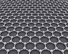
Graphene (/ˈɡræfiːn/[1]) is an allotrope of carbon consisting of a single layer of atoms arranged in a two-dimensional honeycomb lattice[2][3] nanostructure.[4] The name is derived from "graphite" and the suffix -ene, reflecting the fact that the graphite allotrope of carbon contains numerous double bonds.
Each atom in a graphene sheet is connected to its three nearest neighbors by a strong σ-bond, and contributes to a valence band one electron that extends over the whole sheet. This is the same type of bonding seen in carbon nanotubes and polycyclic aromatic hydrocarbons, and (partially) in fullerenes and glassy carbon.[5][6] The valence band is touched by a conduction band, making graphene a semimetal with unusual electronic properties that are best described by theories for massless relativistic particles.[2] Charge carriers in graphene show linear, rather than quadratic, dependence of energy on momentum, and field-effect transistors with graphene can be made that show bipolar conduction. Charge transport is ballistic over long distances; the material exhibits large quantum oscillations and large and nonlinear diamagnetism.[7] Graphene conducts heat and electricity very efficiently along its plane. The material strongly absorbs light of all visible wavelengths,[8][9] which accounts for the black color of graphite; yet a single graphene sheet is nearly transparent because of its extreme thinness. The material is also about 100 times stronger than would be the strongest steel of the same thickness.[10][11]

Scientists theorized the potential existence and production of graphene for decades. It has likely been unknowingly produced in small quantities for centuries, through the use of pencils and other similar applications of graphite. It was possibly observed in electron microscopes in 1962, but studied only while supported on metal surfaces.[12]
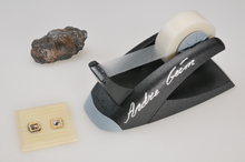
In 2004, the material was rediscovered, isolated and investigated at the University of Manchester,[13][14] by Andre Geim and Konstantin Novoselov. In 2010, Geim and Novoselov were awarded the Nobel Prize in Physics for their "groundbreaking experiments regarding the two-dimensional material graphene".[15] High-quality graphene proved to be surprisingly easy to isolate.
Graphene has become a valuable and useful nanomaterial due to its exceptionally high tensile strength, electrical conductivity, transparency, and being the thinnest two-dimensional material in the world.[4] The global market for graphene was $9 million in 2012,[16] with most of the demand from research and development in semiconductor, electronics, electric batteries,[17] and composites.
The IUPAC (International Union for Pure and Applied Chemistry) recommends use of the name "graphite" for the three-dimensional material, and "graphene" only when the reactions, structural relations or other properties of individual layers are discussed.[18] A narrower definition, of "isolated or free-standing graphene" requires that the layer be sufficiently isolated from its environment,[19] but would include layers suspended or transferred to silicon dioxide or silicon carbide.[20]
History
Structure of graphite and its intercalation compounds
In 1859, Benjamin Brodie noted the highly lamellar structure of thermally reduced graphite oxide.[21][22] In 1916, Peter Debye and Paul Scherrer determined the structure of graphite by powder X-ray diffraction.[23][24][25] The structure was studied in more detail by V. Kohlschütter and P. Haenni in 1918, who also described the properties of graphite oxide paper.[26] Its structure was determined from single-crystal diffraction in 1924.[27][28]
The theory of graphene was first explored by P. R. Wallace in 1947 as a starting point for understanding the electronic properties of 3D graphite. The emergent massless Dirac equation was first pointed out in 1984 separately by Gordon Walter Semenoff,[29] and by David P. DiVincenzo and Eugene J. Mele.[30] Semenoff emphasized the occurrence in a magnetic field of an electronic Landau level precisely at the Dirac point. This level is responsible for the anomalous integer quantum Hall effect.[31][32][33]
Transmission electron microscopy (TEM) images of thin graphite samples consisting of a few graphene layers were published by G. Ruess and F. Vogt in 1948.[34] Eventually, single layers were also observed directly.[35] Single layers of graphite were also observed by transmission electron microscopy within bulk materials, in particular inside soot obtained by chemical exfoliation.[6]
In 1961–1962, Hanns-Peter Boehm published a study of extremely thin flakes of graphite, and coined the term "graphene" for the hypothetical single-layer structure.[36] This paper reports graphitic flakes that give an additional contrast equivalent of down to ~0.4 nm or 3 atomic layers of amorphous carbon. This was the best possible resolution for 1960 TEMs. However, neither then nor today is it possible to argue how many layers were in those flakes. Now we know that the TEM contrast of graphene most strongly depends on focusing conditions.[35] For example, it is impossible to distinguish between suspended monolayer and multilayer graphene by their TEM contrasts, and the only known way is to analyze the relative intensities of various diffraction spots. The first reliable TEM observations of monolayers are probably given in refs. 24 and 26 of Geim and Novoselov's 2007 review.[2]
Starting in the 1970s, C. Oshima and others described single layers of carbon atoms that were grown epitaxially on top of other materials.[37][38] This "epitaxial graphene" consists of a single-atom-thick hexagonal lattice of sp2-bonded carbon atoms, as in free-standing graphene. However, there is significant charge transfer between the two materials, and, in some cases, hybridization between the d-orbitals of the substrate atoms and π orbitals of graphene; which significantly alter the electronic structure compared to that of free-standing graphene.
The term "graphene" was used again in 1987 to describe single sheets of graphite as a constituent of graphite intercalation compounds,[39] which can be seen as crystalline salts of the intercalant and graphene. It was also used in the descriptions of carbon nanotubes by R. Saito and Mildred and Gene Dresselhaus in 1992,[40] and of polycyclic aromatic hydrocarbons in 2000 by S. Wang and others.[41]
Efforts to make thin films of graphite by mechanical exfoliation started in 1990.[42] Initial attempts employed exfoliation techniques similar to the drawing method. Multilayer samples down to 10 nm in thickness were obtained.[2]
In 2002, Robert B. Rutherford and Richard L. Dudman filed for a patent in the US on a method to produce graphene by repeatedly peeling off layers from a graphite flake adhered to a substrate, achieving a graphite thickness of 0.00001 inches (2.5×10⁻⁷ metres). The key to success was high-throughput visual recognition of graphene on a properly chosen substrate, which provides a small but noticeable optical contrast.[43]
Another U.S. patent was filed in the same year by Bor Z. Jang and Wen C. Huang for a method to produce graphene based on exfoliation followed by attrition.[44]
In 2014, inventor Larry Fullerton patents a process for producing single layer graphene sheets.[45]
Full isolation and characterization

Graphene was properly isolated and characterized in 2004 by Andre Geim and Konstantin Novoselov at the University of Manchester.[13][14] They pulled graphene layers from graphite with a common adhesive tape in a process called either micromechanical cleavage or the Scotch tape technique.[46] The graphene flakes were then transferred onto thin silicon dioxide (silica) layer on a silicon plate ("wafer"). The silica electrically isolated the graphene and weakly interacted with it, providing nearly charge-neutral graphene layers. The silicon beneath the SiO
2 could be used as a "back gate" electrode to vary the charge density in the graphene over a wide range.
This work resulted in the two winning the Nobel Prize in Physics in 2010 "for groundbreaking experiments regarding the two-dimensional material graphene."[47][48][46] Their publication, and the surprisingly easy preparation method that they described, sparked a "graphene gold rush". Research expanded and split off into many different subfields, exploring different exceptional properties of the material—quantum mechanical, electrical, chemical, mechanical, optical, magnetic, etc.
Exploring commercial applications
Since the early 2000s, a number of companies and research laboratories have been working to develop commercial applications of graphene. In 2014 a National Graphene Institute was established with that purpose at the University of Manchester, with a 60 million GBP initial funding.[49] In North East England two commercial manufacturers, Applied Graphene Materials[50] and Thomas Swan Limited[51][52] have begun manufacturing. Cambridge Nanosystems[53] is a large-scale graphene powder production facility in East Anglia.
Structure
Bonding
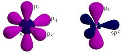
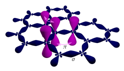
Three of the four outer-shell electrons of each atom in a graphene sheet occupy three sp2 hybrid orbitals – a combination of orbitals s, px and py — that are shared with the three nearest atoms, forming σ-bonds. The length of these bonds is about 0.142 nanometers.[54][55]
The remaining outer-shell electron occupies a pz orbital that is oriented perpendicularly to the plane. These orbitals hybridize together to form two half-filled bands of free-moving electrons, π and π∗, which are responsible for most of graphene's notable electronic properties.[54] Recent quantitative estimates of aromatic stabilization and limiting size derived from the enthalpies of hydrogenation (ΔHhydro) agree well with the literature reports.[56]
Graphene sheets stack to form graphite with an interplanar spacing of 0.335 nm (3.35 Å).
Graphene sheets in solid form usually show evidence in diffraction for graphite's (002) layering. This is true of some single-walled nanostructures.[57] However, unlayered graphene with only (hk0) rings has been found in the core of presolar graphite onions.[58] TEM studies show faceting at defects in flat graphene sheets[59] and suggest a role for two-dimensional crystallization from a melt.
Geometry
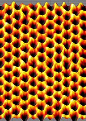
The hexagonal lattice structure of isolated, single-layer graphene can be directly seen with transmission electron microscopy (TEM) of sheets of graphene suspended between bars of a metallic grid[35] Some of these images showed a "rippling" of the flat sheet, with amplitude of about one nanometer. These ripples may be intrinsic to the material as a result of the instability of two-dimensional crystals,[2][60][61] or may originate from the ubiquitous dirt seen in all TEM images of graphene. Photoresist residue, which must be removed to obtain atomic-resolution images, may be the "adsorbates" observed in TEM images, and may explain the observed rippling.[citation needed]
The hexagonal structure is also seen in scanning tunneling microscope (STM) images of graphene supported on silicon dioxide substrates[62] The rippling seen in these images is caused by conformation of graphene to the subtrate's lattice, and is not intrinsic.[62]
Stability
Ab initio calculations show that a graphene sheet is thermodynamically unstable if its size is less than about 20 nm and becomes the most stable fullerene (as within graphite) only for molecules larger than 24,000 atoms.[63]