Quantum dots (QDs) are semiconductor particles a few nanometres in size, having optical and electronic properties that differ from larger particles due to quantum mechanics. They are a central topic in nanotechnology. When the quantum dots are illuminated by UV light, an electron in the quantum dot can be excited to a state of higher energy. In the case of a semiconducting quantum dot, this process corresponds to the transition of an electron from the valence band to the conductance band. The excited electron can drop back into the valence band releasing its energy by the emission of light. This light emission (photoluminescence) is illustrated in the figure on the right. The color of that light depends on the energy difference between the conductance band and the valence band, or transition between discretized energy states when band structure is no longer a good definition in QDs.

In the language of materials science, nanoscale semiconductor materials tightly confine either electrons or electron holes. Quantum dots are sometimes referred to as artificial atoms, emphasizing their singularity, having bound, discrete electronic states, like naturally occurring atoms or molecules.[1][2] It was shown that the electronic wave functions in quantum dots resemble the ones in real atoms.[3] By coupling two or more such quantum dots an artificial molecule can be made, exhibiting hybridization even at room temperature.[4]
Quantum dots have properties intermediate between bulk semiconductors and discrete atoms or molecules. Their optoelectronic properties change as a function of both size and shape.[5][6] Larger QDs of 5–6 nm diameter emit longer wavelengths, with colors such as orange or red. Smaller QDs (2–3 nm) emit shorter wavelengths, yielding colors like blue and green. However, the specific colors vary depending on the exact composition of the QD.[7]
Potential applications of quantum dots include single-electron transistors, solar cells, LEDs, lasers,[8] single-photon sources,[9][10][11] second-harmonic generation, quantum computing,[12] cell biology research,[13] microscopy,[14] and medical imaging.[15] Their small size allows for some QDs to be suspended in solution, which may lead to use in inkjet printing and spin-coating.[16] They have been used in Langmuir-Blodgett thin-films.[17][18][19] These processing techniques result in less expensive and less time-consuming methods of semiconductor fabrication.
Production

There are several ways to fabricate quantum dots. Possible methods include colloidal synthesis, self-assembly, and electrical gating.
Colloidal synthesis
Colloidal semiconductor nanocrystals are synthesized from solutions, much like traditional chemical processes. The main difference is the product neither precipitates as a bulk solid nor remains dissolved.[5] Heating the solution at high temperature, the precursors decompose forming monomers which then nucleate and generate nanocrystals. Temperature is a critical factor in determining optimal conditions for the nanocrystal growth. It must be high enough to allow for rearrangement and annealing of atoms during the synthesis process while being low enough to promote crystal growth. The concentration of monomers is another critical factor that has to be stringently controlled during nanocrystal growth. The growth process of nanocrystals can occur in two different regimes, "focusing" and "defocusing". At high monomer concentrations, the critical size (the size where nanocrystals neither grow nor shrink) is relatively small, resulting in growth of nearly all particles. In this regime, smaller particles grow faster than large ones (since larger crystals need more atoms to grow than small crystals) resulting in the size distribution focusing, yielding an improbable distribution of nearly monodispersed particles. The size focusing is optimal when the monomer concentration is kept such that the average nanocrystal size present is always slightly larger than the critical size. Over time, the monomer concentration diminishes, the critical size becomes larger than the average size present, and the distribution defocuses.

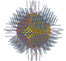
There are colloidal methods to produce many different semiconductors. Typical dots are made of binary compounds such as lead sulfide, lead selenide, cadmium selenide, cadmium sulfide, cadmium telluride, indium arsenide, and indium phosphide. Dots may also be made from ternary compounds such as cadmium selenide sulfide. Further, recent advances have been made which allow for synthesis of colloidal perovskite quantum dots.[20] These quantum dots can contain as few as 100 to 100,000 atoms within the quantum dot volume, with a diameter of ≈10 to 50 atoms. This corresponds to about 2 to 10 nanometers, and at 10 nm in diameter, nearly 3 million quantum dots could be lined up end to end and fit within the width of a human thumb.
Large batches of quantum dots may be synthesized via colloidal synthesis. Due to this scalability and the convenience of benchtop conditions, colloidal synthetic methods are promising for commercial applications.
Plasma synthesis
Plasma synthesis has evolved to be one of the most popular gas-phase approaches for the production of quantum dots, especially those with covalent bonds.[21][22][23] For example, silicon (Si) and germanium (Ge) quantum dots have been synthesized by using nonthermal plasma. The size, shape, surface and composition of quantum dots can all be controlled in nonthermal plasma.[24][25] Doping that seems quite challenging for quantum dots has also been realized in plasma synthesis.[26][27][28] Quantum dots synthesized by plasma are usually in the form of powder, for which surface modification may be carried out. This can lead to excellent dispersion of quantum dots in either organic solvents[29] or water[30] (i. e., colloidal quantum dots).
Fabrication
- Self-assembled quantum dots are typically between 5 and 50 nm in size. Quantum dots defined by lithographically patterned gate electrodes, or by etching on two-dimensional electron gases in semiconductor heterostructures can have lateral dimensions between 20 and 100 nm.
- Some quantum dots are small regions of one material buried in another with a larger band gap. These can be so-called core–shell structures, e.g., with CdSe in the core and ZnS in the shell, or from special forms of silica called ormosil. Sub-monolayer shells can also be effective ways of passivating the quantum dots, such as PbS cores with sub-monolayer CdS shells.[31]
- Quantum dots sometimes occur spontaneously in quantum well structures due to monolayer fluctuations in the well's thickness.
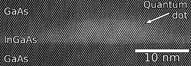
- Self-assembled quantum dots nucleate spontaneously under certain conditions during molecular beam epitaxy (MBE) and metalorganic vapour-phase epitaxy (MOVPE), when a material is grown on a substrate to which it is not lattice matched. The resulting strain leads to the formation of islands on top of a two-dimensional wetting layer. This growth mode is known as Stranski–Krastanov growth.[32] The islands can be subsequently buried to form the quantum dot. A widely used type of quantum dots grown with this method are indium gallium arsenide (InGaAs) quantum dots in gallium arsenide (GaAs).[33] Such quantum dots have the potential for applications in quantum cryptography (i.e. single photon sources) and quantum computation. The main limitations of this method are the cost of fabrication and the lack of control over positioning of individual dots.
- Individual quantum dots can be created from two-dimensional electron or hole gases present in remotely doped quantum wells or semiconductor heterostructures called lateral quantum dots. The sample surface is coated with a thin layer of resist. A lateral pattern is then defined in the resist by electron beam lithography. This pattern can then be transferred to the electron or hole gas by etching, or by depositing metal electrodes (lift-off process) that allow the application of external voltages between the electron gas and the electrodes. Such quantum dots are mainly of interest for experiments and applications involving electron or hole transport, i.e., an electrical current.
- The energy spectrum of a quantum dot can be engineered by controlling the geometrical size, shape, and the strength of the confinement potential. Also, in contrast to atoms, it is relatively easy to connect quantum dots by tunnel barriers to conducting leads, which allows the application of the techniques of tunneling spectroscopy for their investigation.
The quantum dot absorption features correspond to transitions between discrete, three-dimensional particle in a box states of the electron and the hole, both confined to the same nanometer-size box. These discrete transitions are reminiscent of atomic spectra and have resulted in quantum dots also being called artificial atoms.[34]
- Confinement in quantum dots can also arise from electrostatic potentials (generated by external electrodes, doping, strain, or impurities).
- Complementary metal-oxide-semiconductor (CMOS) technology can be employed to fabricate silicon quantum dots. Ultra small (L=20 nm, W=20 nm) CMOS transistors behave as single electron quantum dots when operated at cryogenic temperature over a range of −269 °C (4 K) to about −258 °C (15 K). The transistor displays Coulomb blockade due to progressive charging of electrons (holes) one by one. The number of electrons (holes) confined in the channel is driven by the gate voltage, starting from an occupation of zero electrons (holes), and it can be set to 1 or many.[35]
Viral assembly
Genetically engineered M13 bacteriophage viruses allow preparation of quantum dot biocomposite structures.[36] It had previously been shown that genetically engineered viruses can recognize specific semiconductor surfaces through the method of selection by combinatorial phage display.[37] Additionally, it is known that liquid crystalline structures of wild-type viruses (Fd, M13, and TMV) are adjustable by controlling the solution concentrations, solution ionic strength, and the external magnetic field applied to the solutions. Consequently, the specific recognition properties of the virus can be used to organize inorganic nanocrystals, forming ordered arrays over the length scale defined by liquid crystal formation. Using this information, Lee et al. (2000) were able to create self-assembled, highly oriented, self-supporting films from a phage and ZnS precursor solution. This system allowed them to vary both the length of bacteriophage and the type of inorganic material through genetic modification and selection.
Electrochemical assembly
Highly ordered arrays of quantum dots may also be self-assembled by electrochemical techniques. A template is created by causing an ionic reaction at an electrolyte-metal interface which results in the spontaneous assembly of nanostructures, including quantum dots, onto the metal which is then used as a mask for mesa-etching these nanostructures on a chosen substrate.[citation needed]
Bulk-manufacture
Quantum dot manufacturing relies on a process called high temperature dual injection which has been scaled by multiple companies for commercial applications that require large quantities (hundreds of kilograms to tonnes) of quantum dots. This reproducible production method can be applied to a wide range of quantum dot sizes and compositions.
The bonding in certain cadmium-free quantum dots, such as III-V-based quantum dots, is more covalent than that in II-VI materials, therefore it is more difficult to separate nanoparticle nucleation and growth via a high temperature dual injection synthesis. An alternative method of quantum dot synthesis, the molecular seeding process, provides a reproducible route to the production of high-quality quantum dots in large volumes. The process utilises identical molecules of a molecular cluster compound as the nucleation sites for nanoparticle growth, thus avoiding the need for a high temperature injection step. Particle growth is maintained by the periodic addition of precursors at moderate temperatures until the desired particle size is reached.[38] The molecular seeding process is not limited to the production of cadmium-free quantum dots; for example, the process can be used to synthesise kilogram batches of high-quality II-VI quantum dots in just a few hours.
Another approach for the mass production of colloidal quantum dots can be seen in the transfer of the well-known hot-injection methodology for the synthesis to a technical continuous flow system. The batch-to-batch variations arising from the needs during the mentioned methodology can be overcome by utilizing technical components for mixing and growth as well as transport and temperature adjustments. For the production of CdSe based semiconductor nanoparticles this method has been investigated and tuned to production amounts of kg per month. Since the use of technical components allows for easy interchange in regards of maximum throughput and size, it can be further enhanced to tens or even hundreds of kilograms.[39]
In 2011 a consortium of U.S. and Dutch companies reported a milestone in high volume quantum dot manufacturing by applying the traditional high temperature dual injection method to a flow system.[40]
On 23 January 2013 Dow entered into an exclusive licensing agreement with UK-based Nanoco for the use of their low-temperature molecular seeding method for bulk manufacture of cadmium-free quantum dots for electronic displays, and on 24 September 2014 Dow commenced work on the production facility in South Korea capable of producing sufficient quantum dots for "millions of cadmium-free televisions and other devices, such as tablets". Mass production is due to commence in mid-2015.[41] On 24 March 2015 Dow announced a partnership deal with LG Electronics to develop the use of cadmium free quantum dots in displays.[42]
Heavy-metal-free quantum dots
In many regions of the world there is now a restriction or ban on the use of heavy metals in many household goods, which means that most cadmium-based quantum dots are unusable for consumer-goods applications.
For commercial viability, a range of restricted, heavy-metal-free quantum dots has been developed showing bright emissions in the visible and near-infrared region of the spectrum and have similar optical properties to those of CdSe quantum dots. Among these materials are InP/ZnS, CuInS/ZnS, Si, Ge and C.
Peptides are being researched as potential quantum dot material.[43]
Health and safety
Some quantum dots pose risks to human health and the environment under certain conditions.[44][45][46] Notably, the studies on quantum dot toxicity have focused on particles containing cadmium and have yet to be demonstrated in animal models after physiologically relevant dosing.[46] In vitro studies, based on cell cultures, on quantum dots (QD) toxicity suggest that their toxicity may derive from multiple factors including their physicochemical characteristics (size, shape, composition, surface functional groups, and surface charges) and their environment. Assessing their potential toxicity is complex as these factors include properties such as QD size, charge, concentration, chemical composition, capping ligands, and also on their oxidative, mechanical and photolytic stability.[44]
Many studies have focused on the mechanism of QD cytotoxicity using model cell cultures. It has been demonstrated that after exposure to ultraviolet radiation or oxidation by air, CdSe QDs release free cadmium ions causing cell death.[47] Group II–VI QDs also have been reported to induce the formation of reactive oxygen species after exposure to light, which in turn can damage cellular components such as proteins, lipids and DNA.[48] Some studies have also demonstrated that addition of a ZnS shell inhibits the process of reactive oxygen species in CdSe QDs. Another aspect of QD toxicity is that there are, in vivo, size-dependent intracellular pathways that concentrate these particles in cellular organelles that are inaccessible by metal ions, which may result in unique patterns of cytotoxicity compared to their constituent metal ions.[49] The reports of QD localization in the cell nucleus[50] present additional modes of toxicity because they may induce DNA mutation, which in turn will propagate through future generation of cells, causing diseases.
Although concentration of QDs in certain organelles have been reported in in vivo studies using animal models, no alterations in animal behavior, weight, hematological markers or organ damage has been found through either histological or biochemical analysis.[51] These findings have led scientists to believe that intracellular dose is the most important determining factor for QD toxicity. Therefore, factors determining the QD endocytosis that determine the effective intracellular concentration, such as QD size, shape and surface chemistry determine their toxicity. Excretion of QDs through urine in animal models also have demonstrated via injecting radio-labeled ZnS-capped CdSe QDs where the ligand shell was labelled with 99mTc.[52] Though multiple other studies have concluded retention of QDs in cellular levels,[46][53] exocytosis of QDs is still poorly studied in the literature.
While significant research efforts have broadened the understanding of toxicity of QDs, there are large discrepancies in the literature, and questions still remain to be answered. Diversity of this class of material as compared to normal chemical substances makes the assessment of their toxicity very challenging. As their toxicity may also be dynamic depending on the environmental factors such as pH level, light exposure and cell type, traditional methods of assessing toxicity of chemicals such as LD50 are not applicable for QDs. Therefore, researchers are focusing on introducing novel approaches and adapting existing methods to include this unique class of materials.[46] Furthermore, novel strategies to engineer safer QDs are still under exploration by the scientific community. A recent novelty in the field is the discovery of carbon quantum dots, a new generation of optically-active nanoparticles potentially capable of replacing semiconductor QDs, but with the advantage of much lower toxicity.
Optical properties

In semiconductors, light absorption generally leads to an electron being excited from the valence to the conduction band, leaving behind a hole. The electron and the hole can bind to each other to form an exciton. When this exciton recombines (i.e. the electron resumes its ground state), the exciton's energy can be emitted as light. This is called fluorescence. In a simplified model, the energy of the emitted photon can be understood as the sum of the band gap energy between the highest occupied level and the lowest unoccupied energy level, the confinement energies of the hole and the excited electron, and the bound energy of the exciton (the electron–hole pair):

As the confinement energy depends on the quantum dot's size, both absorption onset and fluorescence emission can be tuned by changing the size of the quantum dot during its synthesis. The larger the dot, the redder (lower energy) its absorption onset and fluorescence spectrum. Conversely, smaller dots absorb and emit bluer (higher energy) light. Recent articles in Nanotechnology and in other journals have begun to suggest that the shape of the quantum dot may be a factor in the coloration as well, but as yet not enough information is available. Furthermore, it was shown[54] that the lifetime of fluorescence is determined by the size of the quantum dot. Larger dots have more closely spaced energy levels in which the electron–hole pair can be trapped. Therefore, electron–hole pairs in larger dots live longer causing larger dots to show a longer lifetime.
To improve fluorescence quantum yield, quantum dots can be made with shells of a larger bandgap semiconductor material around them. The improvement is suggested to be due to the reduced access of electron and hole to non-radiative surface recombination pathways in some cases, but also due to reduced Auger recombination in others.